
Optical products are actually very common in our lives, as simple as the glasses we wear, as well as small-caliber applications such as camera lenses and security cameras, to optical lenses for remote sensing imaging satellites, astronomical telescopes (Hubble, Weber) mirrors, Large-caliber fields such as large optical telescopes, weapon photoelectric pod lenses, etc. We are constantly enriching our products and expanding their application fields. Technological breakthroughs enable us to constantly challenge the limits of craftsmanship and meet more demanding and stricter application scenarios. The optical industry relies on mechanical components of utmost precision and accuracy to ensure their seamless integration into sophisticated equipment like lasers, cameras, microscopes, and telescopes. End users of these products demand high levels of accuracy to support their specific optical solutions.
Optical product manufacturers in the optics industry often face significant challenges due to the extremely tight tolerances, demanding quality control standards, and the need for visually appealing aesthetics. However, our expertise and cutting-edge machinery position us well to tackle these challenges. We are well-versed in the challenging manufacturing requirements involved in the optical industry, including fine threading, precise positioning, and superior surface finishes.
At Be-Cu prototype, we consistently assist our customers in designing custom optical components in compliance with specific requirements and specifications. Our skilled machinists well comprehend how each component fits within the overall project and its intended application, enabling them to effectively machine parts that perfectly fit into the assembly.The market demand is constantly promoting people to iteratively update technology creation Produce more and more incredible products. So today we will briefly talk about the knowledge about optical machining, how an inconspicuous raw material turns into various products and equipment in our hands, and what kind of process it is.
Process flow of precision optical machining: How does a material become an optical product?
First of all, let’s visually see how raw materials are transformed into optical component products step by step from the figure below.
The optical machining technology mainly includes blank forming, rough grinding, fine grinding, polishing, edging, coating, gluing and other process links. Optical raw materials: optical glass: including colored optical glass, laser glass, quartz optical glass, anti-radiation glass, ultraviolet infrared optical glass, fiber optic glass, acousto-optic glass, magneto-optical glass and photochromic glass.
Optical crystal:
- Halide single crystal: fluoride single crystal, bromine, chlorine, iodine compound single crystal, thallium halide single crystal.
- Oxide single crystals: sapphire (Al2O3), crystal (SiO2), magnesia (MgO) and rutile (TiO2), compared with halide single crystals, have a high melting point and good chemical stability, in the visible and near-infrared spectral regions Good permeability. Used in the manufacture of various optical components from the ultraviolet to the infrared spectral region.
- Semiconductor crystals: single crystals (such as germanium single crystals, silicon single crystals), II-VI semiconductor single crystals, III-V semiconductor single crystals and diamond. Diamond is the crystal with the longest spectral transmission band, which can be extended to the far infrared region, and has a high melting point, high hardness, excellent physical properties and chemical stability. Semiconductor single crystals can be used as infrared window materials, infrared filters and other optical components.
- Optical plastics: polymethyl methacrylate (PMMA), polystyrene (PS), polycarbonate (PC), styrene acrylonitrile is often abbreviated as AS and SAN, styrene-methyl methacrylate copolymer (MS ), poly-4-methyl-1-pentene, referred to as TPX, trade name TPX, transparent polyamide.
Blank forming:
Raw materials made from the most primitive ores or chemical reactions need to be preliminarily processed before they enter the formal machining, and these materials are processed into the prototypes that we need for subsequent machining, which is called the blank forming process. Blanks are the initial form of optical parts, including block blanks (for small batches), profile blanks (large batches), and bar blanks.
Glass block blank forming:
It is a blank processed from glass blocks. There are many processes under the blank forming process, the main machining procedures are: sawing, leveling, scoring, rounding, and opening the ball.
- Sawing: The machining of glass optical material blanks mainly adopts diamond sawing machines. According to the characteristics of the feeder, it can be divided into three types: hammer feed, screw feed and hydraulic feed.
- Leveling: Grinding the uneven surface of the billet after sawing, and grinding the thickness, the parallelism of the two sides, the grinding angle, etc., there are two kinds of loose abrasive grinding and diamond grinding wheel milling.
- Scribing and cutting: Cut the blanks that need to be used and remove the excess parts. Diamond glass knife (or hob) is often used for scribing and cutting.
- Rounding: The blank of a round part is flattened and turned into a long strip for grinding the outer circle, which is called rounding. The commonly used methods are: rounding with loose grain abrasives on a flat grinding disc; grinding the outer circle with a grinding wheel on an outer cylindrical grinder.
- Open spherical surface: The open spherical surface of the blank of the lens is to grind the rounded blank into a spherical surface, which can meet the requirements of the radius of curvature and center thickness after the rough grinding of the part, so the open spherical surface can be a kind of rough grinding. There are two main methods: loose grain abrasive grinding and diamond grinding wheel milling.
- Plastic blank forming:The blank machining methods of optical glass parts include: hot pressing molding, casting molding and other methods. The main process of hot pressing blanks includes: material preparation, heating, pressing and annealing.
- Bar stock forming:The general process of producing blanks from bar stock is: cutting and opening.
- Coarse grinding:The process of machining blocks or profile blanks into a certain geometric shape, dimensional accuracy and surface roughness. Coarse grinding methods include loose abrasive machining and fixed abrasive machining.
Scattered abrasive machining: the rough machining of glass workpieces on the grinding disc with abrasives stirred with emery and water. According to the shape of the ball mill, it can be divided into concave ball mill for grinding convex parts and convex ball mill for concave parts. Under this machining method, the rough grinding spherical surface generally needs to be processed with three abrasives from coarse to fine. The choice of the first abrasive particle size should be determined according to the arc height of the workpiece: when the single arc height is greater than 1mm, the first abrasive grain size is coarser than 180#; when the single arc height is 0.4-1mm, choose 180# abrasive; When the arc height of a single piece is less than 0.4mm, use 240# or 280# abrasive. The strength of the second and third rough grinding abrasives should be 1 or 2 smaller than that of the first abrasive. After rough grinding, the surface roughness is required to reach 1.6μm, which is equivalent to the surface processed by W40 or W28 abrasives.
Fixed abrasive machining: the mechanical crushing and removal process of sharp and hard abrasive particles on the glass surface, and the hydrolysis is secondary.
Rough grinding of spherical surface: Washing machining is usually used for rough grinding of spherical surface, also known as Fancheng method, which is a method of forming a spherical surface by using the enveloping surface of the grinding wheel cutting edge track. It is a fixed abrasive machining method.
Fine grinding:
Reduce the depth of the concave-convex layer on the surface of the part and improve its uniformity; further improve the surface shape accuracy and related dimensional accuracy of the part surface to meet the requirements of polishing on the surface structure and shape of the part.
Fine grinding generally uses two sands, that is, two abrasives with different particle sizes. If the abrasive grain size of the first sand is W28, the abrasive grain size of the second sand is W14. Some special parts require three or four sands, and the abrasive grain size can be W28, W14, W10, W7, etc.
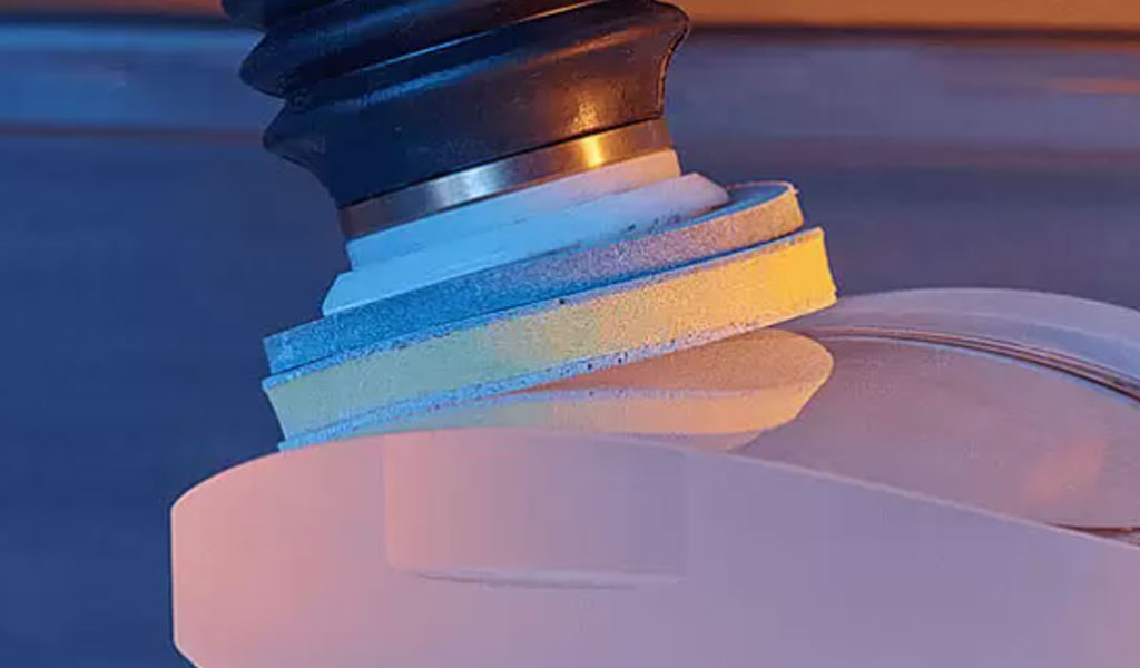
Polishing:
Polishing is the link that has the greatest impact on the accuracy of optical components, or in other words, polishing plays an absolutely important role in improving the accuracy of optical components. Because polishing is the last and most important process of surface machining of optical components.
There are two main purposes of polishing: remove the damaged layer of fine grinding to meet the specified surface defect grade requirements; refine the surface shape to meet the aperture and local aperture number required by the drawing to form a smooth and transparent surface.
From the point of view of its importance, it directly affects the accuracy of components, which involves many key and core technologies, so this part of the work is basically in the hands of the manufacturer itself, and the quality is controllable. Therefore, we will introduce polishing separately in the following sections.
Edging (centering edging):
There are special requirements for the edge shape or the lens whose edge part is within the use range needs to be edged, and the centered lens should be symmetrically ground to the outer circle.
Ultrasonic cleaning:
The optical components are cleaned after surface machining to facilitate subsequent processes.
Coating:
One of the important technologies involved in the manufacture of ultra-precision optical devices is surface coating technology. The spectroscopic properties of optical components are realized by the polarization splitting, anti-reflection, and accurate positioning of spectral wavelengths of optical films.
Precision optical components have high requirements on the spectral control ability and precision of optical thin films, and the design of optical thin films is becoming more and more complex. The number of layers of optical thin films required for high performance has reached more than 100 layers, and there are ultra-thin layers with a thickness of only a few nanometers. A stable coating process and monitoring technology are key factors to ensure high-quality optical films.
Therefore, this part of the process is still completed in the hands of the optical manufacturer itself, and together with polishing, it has become the two most important links in the entire optical machining link.
Glued:
The gluing process of optical lenses refers to the process of bonding two or more lenses and plane mirrors to form optical components according to certain technical requirements by using optical glue or optical glue on the optical surfaces that match each other. The purpose is to improve the image quality; reduce the loss of reflected light energy; simplify the machining of complex parts; protect the scoring surface.
Methods: resin glue method, light glue method; mechanical glue method.
Assembly:
Mount the fabricated optical components on specific mechanical accessories (if necessary). Then there is packaging into bags and storage of finished products, so I won’t introduce too much here.
The process described above is a relatively common process, and some optical components do not need to have all the processes, such as single-layer lenses and single-layer optical components, there is no need to consider the gluing process. For different application scenarios, the specific processes corresponding to different products are slightly different, and the machining technologies involved are also different.
In some relatively simple or less demanding links in the entire machining process, manufacturers usually choose outsourced machining. For example, simple machining procedures such as optical lens blank cutting and drilling in the process of cold machining optical devices; medium and low difficulty coatings mainly include conventionally required antireflection coatings, ordinary energy splitting coatings, and general narrow-band filter coatings. The process requirements are not high.
For the important links that affect the machining of components: polishing (high-precision flat, spherical, aspheric, cylindrical polishing, etc.) and coating (high-precision, high-performance coating), optical manufacturers generally invest in their own equipment to facilitate quality control.
One of the important links that affect machining accuracy and product performance: polishing
In the previous section, we introduced the role of polishing, using high-precision polishing equipment to refine the surface of optical components to remove surface defects and keep the surface smooth.
Traditional equipment for machining optical components mainly includes single-axis machines, multi-axis machines, flat-spherical machines, and separators. These traditional machining methods mainly rely on the experience of optical processors, and have low machining efficiency, long machining cycles, and unstable quality. The disadvantage is that it is difficult to process optical components to high precision.
With the development of computer technology, computer-controlled optical surface shaping technology (Computer Controlled Optical Surfacing, CCOS, generally using small grinding head polishing tools) has gradually entered industrial applications. Subsequently, some other polishing methods were developed on the basis of CCOS technology, such as stress disk polishing, airbag polishing, magnetorheological polishing and ion beam machining methods.
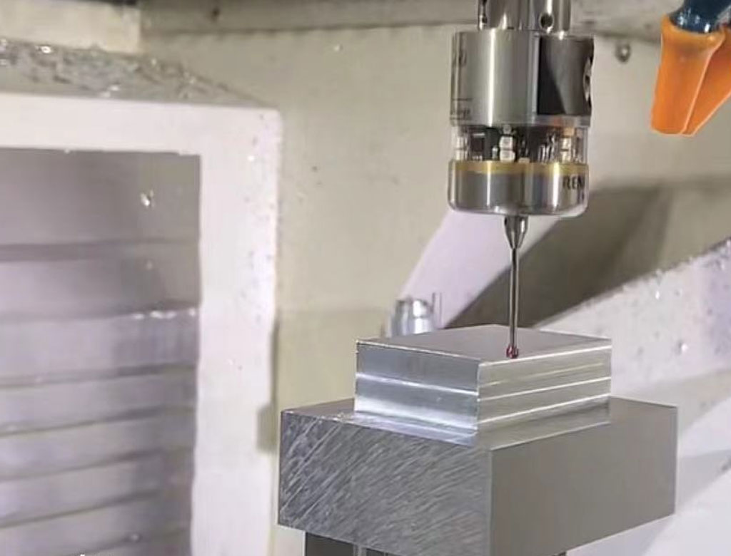
Among these methods, ion beam polishing has the highest machining accuracy, and is the final process of improving the surface shape of optical components. It can be said that the accuracy of ion beam machining determines the highest precision of optical components. Ion beam machining has been widely used in In the field of cnc machining optical parts, its high-precision and high-efficiency characteristics have strong advantages, especially in the machining of large-diameter optical components.
Below we introduce these technologies separately.
Small grinding head polishing technology:
A grinding head much smaller than the diameter of the workpiece is used to polish the workpiece, and the amount of material removal is controlled by controlling the residence time of the grinding head at different positions on the surface of the workpiece and the pressure between the grinding head and the workpiece.
This technology was first proposed by the Itek company in the United States, and it was gradually applied in industrial manufacturing later. The typical American Hubble Space Telescope primary mirror with a diameter of 2.4m is polished by CCOS, and the final surface shape accuracy reaches 12nm RMS.
Due to the use of computer control instead of manual experience, the small grinding head technology makes optical processing get rid of traditional manual polishing. The polishing process is stable and has high certainty. Therefore, the processing efficiency and processing accuracy are also high, which can greatly shorten the processing cycle of large-diameter optical components. .
At the same time, the principle of small grinding head technology is simple, low cost, easy to implement, and different sizes of grinding heads can be replaced according to actual needs, so it has been widely used in the processing of large-diameter optical components.
However, the small grinding head technology is still contact machining, which has some disadvantages such as edge effect, polishing disc wear and sub-surface damage. At the same time, because the polishing disc is a rigid disc, it cannot fit the mirror surface well when processing aspheric surfaces, which is easy produce medium and high frequency errors.
Stressed Lap Polishing (SLP):
An aspheric surface processing method developed according to the principle of thin plate stress deformation. When polishing an aspheric workpiece, the shape of the stress disk can be changed into the required surface shape in real time through computer control, and the complete adhesion between the polishing disk and the mirror surface of the workpiece can be realized. combine. SLP overcomes the disadvantage that the small grinding head polishing disc is a rigid disc that cannot completely match the aspheric surface, and is a development and supplement to the small grinding head technology.
This technology was proposed in the early 1990s by the Large Mirror Laboratory of the Stilva Observatory at the University of Arizona. And successfully developed the stress disc polishing machine tool, which can process the workpiece diameter up to Φ8.0m, and the effective diameter of the stress disc is Φ1.2m. Using this equipment, a series of large mirrors have been processed, including: 1.8mf/1.0 VATT primary mirror (Lennon Telescope) , 3.5mf/1.5 SOR primary mirror, 6.5mf/1.25 Multiple Mirror Telescope (MMT) primary mirror and 6.5mf/1.25 Magellan primary mirror.
Compared with the small grinding head technology, the SLP technology is more suitable for processing large-diameter optical elements due to the larger diameter of the stress disc and high removal efficiency, and when processing aspheric surfaces, the grinding head can closely fit the surface of the workpiece, so it will not produce medium and high frequency errors. However, since SLP technology, like small grinding head technology, is also a contact processing method, it also has disadvantages such as edge effects and subsurface damage.
In addition, since the surface shape of the stress disk is required to change in real time according to the shape of the workpiece when processing an aspheric surface, the requirements for control technology are also high.
Magnetorheological finishing (MRF):
In the early 1990s, the COM Center of the United States proposed this technology, which combined the theory of electromagnetism and fluid mechanics, and used the rheological properties of magnetorheological fluid in a magnetic field to polish optical components.
MRF does not have a polishing disc, and uses the shear force between the magnetorheological fluid and the workpiece to remove material, and the positive pressure on the workpiece is very small, so there are no disadvantages such as polishing disc wear and subsurface damage in the contact polishing method.
However, due to the large size of the MRF polishing wheel, the removal efficiency is sensitive to the polishing distance, so it is not suitable for polishing high-steep concave surfaces and large long-diameter inner cavity components.
Balloon Polishing Technology (Bonnet Polishing):
A special flexible airbag with online controllable air pressure is used. The shape of the airbag is a spherical crown, and a special flexible polyurethane polishing pad or polishing cloth is pasted on the outside of the airbag.
This technology was proposed by the Optical Laboratory of the University of London in the 1990s, with the purpose of solving the situation that the aspheric surface processing polishing disc does not match the aspheric surface shape.
The airbag is a flexible structure, which can fit the workpiece well; the material removal in the polishing area is uniform; the process controllability is good, etc. Therefore, this method is easy to process optical devices with high precision and high surface quality. In recent years, the development direction of airbag polishing technology is to improve processing efficiency, reduce edge effects and remove medium and high frequency errors.
Ion Beam Figuring (IBF):
Under vacuum conditions, inert gases such as argon (Ar), krypton (Kr), and xenon (Xe) are ionized through the ion source to generate an ion beam with a certain energy to bombard the surface of the workpiece. When the ion beam reaches the surface of the workpiece, It will exchange energy with the workpiece material atoms. When the surface atoms of the workpiece get enough energy to get rid of the binding energy of the material surface, they will break away from the surface of the workpiece, thereby realizing the removal of the material.
As early as 1965, American Meinel discovered that optical materials were removed under the action of ion beams, but because the energy density of the narrow-beam high-energy ion source used at that time was too high, the mirror was burned in a short time, and it was difficult to control the energy. Emissive density, the efficiency of processing removal is very low, so there is no progress in use for a long time. Until the late 1970s, the emergence of wide-beam and low-energy Kaufman ion sources made this technology available, which not only limited the ion energy to the range of 300-1500eV, did not cause damage to the optical mirror, but also improved The efficiency of ion beam processing, so ion beam technology began to be formally applied to the processing of optical components.
Ion beam polishing technology has the following advantages:
- Non-contact processing: The ion beam has no mechanical force on the surface of the workpiece during processing, so it will not cause subsurface damage to the workpiece. At the same time, the shape and removal efficiency of the removal function will not change at the edge of the workpiece, so there is no edge effect.
High processing precision and good surface finish: Processing is carried out under the precise control of computer and interferometer, theoretically the processing accuracy can reach atomic level, the processing environment is stable, the ion beam generated by the ion source has small fluctuations, and the surface of the workpiece will not wear. - Gaussian removal function: Compared with several other polishing methods, the removal function is closest to the Gaussian distribution, which is convenient for solving the residence time distribution.
- The robustness of the removal function is good: the ion beam polishing is in a vacuum, the controllability and stability of the removal function are good, and it is suitable for processing large-aperture optical components;
- Wide applicability of surface shape: During ion beam polishing, the ion beam flow is always in close contact with the surface of the workpiece, and there will be no medium and high frequency errors caused by the mismatch between the polishing tool and the mirror surface, so it is suitable for the processing of spherical and aspherical surfaces, especially It is a high-precision machining of high-steep aspheric surfaces;
- Wide range of application materials: processing materials generally include metals, ceramics, and precious stones, typically 316L stainless steel, AZI magnesium alloy, high-temperature alloy, high-speed steel, W6M05Cr4V2 high-speed steel, composite nitride hard coating, and DLC.
Summarize:
For large-aperture optical elements with high requirements for surface shape accuracy, it is still difficult to process them to high precision by only a single method. Generally, it is necessary to select different processing methods in combination according to the magnitude and frequency band distribution of surface shape residuals during the processing process. . When the residual error of the surface shape is small and close to the target value, ion beam polishing is used for final high-precision polishing.
Judgment of excellent processing ability: a brief analysis of key processes and indicators
We have mentioned many relevant figures and indicators in the process of introducing different processing technologies above. Here we will briefly introduce some important influencing indicators.
Processing type:
- Aspheric surface processing: Broadly speaking, aspheric surfaces are other surfaces that do not include spherical surfaces and planes. From the perspective of application, aspheric surfaces can be divided into axisymmetric aspheric surfaces, aspheric surfaces with two symmetrical surfaces, and aspheric surfaces without symmetrical surfaces. free-form surfaces (spectacles lenses). The difficulty of processing an aspheric surface is that there is no fixed general function expression on its surface. The spherical functions corresponding to different application scenarios may be different, which can be called free-form surfaces. Free-form surfaces can generally be expressed through polynomial series, Zernike series or Cubic spline interpolation is described, which is similar to the cumulative approximation of multiple small areas on the surface. It is also a concept of limit, and each point needs to be solved when writing a program.
- Spherical surface processing: Simply put, the surface to be processed is a hemispherical surface or a spherical arc surface with regular surface functions. When performing milling, polishing and other processes, the setting of the grinding head or polishing surface is relatively easy, and a good adhesion can be maintained. The degree of processing is relatively low.
- Cylindrical surface processing: Cylindrical lens is a common type of aspheric lens. The intersection lines of the cylindrical lens and the meridional and sagittal sections are respectively the intersection line of two circular arcs and two parallel straight lines. Description, one section has optical power, while the other section has no optical power. When a parallel laser beam passes through the cylindrical mirror, the focal point can be drawn into a line along one direction. This cylindrical mirror Attributes have their specific uses in some special cases. For example, it has a wide range of applications in linear detector illumination, barcode scanning, holographic illumination, optical information processing, computers, laser emission, intense laser systems, and synchrotron radiation beamlines.
Technical indicators:
Processing diameter: mainly for the processing of aspheric surfaces. Aspheric surfaces cannot be measured by the radius of a spherical or cylindrical surface. Therefore, the diameter of the processed surface is directly used for analysis, usually ranging from mm to m. The larger the processing diameter means the larger the size of the processing surface. Under certain precision requirements, it has higher requirements for large grinding heads or high-efficiency ion beams. The larger the diameter, the same precision, the lower the processing efficiency; the larger the diameter, the same processing efficiency, the lower the precision. How to ensure high efficiency and high precision when facing large-diameter or large-caliber processing is an important trend and direction of optical processing.
Surface accuracy:
PV: Peak to Valley, PV=Wmax-Wmin, in simple terms, is the height difference between the highest point and the lowest point on the processed surface (usually in um), there are subtle differences for spherical, flat and aspheric surfaces Define the difference. Due to the difference in the spatial resolution of the detectors used in the current interferometer detection equipment, noise, bright spots, etc. will have a relatively large impact, so PV is sometimes larger than the real data, so PVr is sometimes used to describe the surface shape precision. Regardless of the PV or PVr value, the larger the value, the rougher the surface.
RMS: Root mean square, root mean square, the following is its calculation formula. It can be seen from the formula that it represents an average value of all bumps on the surface. If the PV value represents the maximum height difference on the entire surface, then the RMS represents the average value of all height differences on the surface, and the smaller the RMS, the smoother the surface. Therefore, it can be seen that the smaller the PV value does not necessarily mean the higher the accuracy of the surface shape, and the value of RMS must be taken into account. It’s like a point that fluctuates around the mean line of error.
Surface finish: Two sets of numbers are usually used to indicate the size of surface defects, for example, 40/20, 40 represents the size of surface limited scratches, and 20 represents the size of surface defect pits. The smaller the value of the two, the higher the requirement for surface finish. (Aspect ratio > 4:1 is scratches, < 4:1 is pitting).
Busbar offset: This index is usually listed separately in cylindrical surface processing, and the cylindrical surface can be regarded as a structure formed by rotating the plane around the busbar.
Regarding technical indicators, the ideal state is to achieve the ultimate in each indicator. But in reality, it is a process of compatibility and compromise. For example, when facing large-caliber processing, if you want to improve a certain processing efficiency, you may face the loss of part of the processing accuracy; when you want to improve the overall processing accuracy, It is necessary to reduce the processing efficiency to a certain extent (the higher the processing accuracy, the more iterative processing times, and the greater the time cost). Indicators of this type need to be considered in compromise.
There is another type of indicators that are biased towards each other. For example, the PV and RMS mentioned above are not the best for a single indicator. Another indicator must be able to do it. The smaller the PV value does not mean the better the surface. Evenly, to some extent, the proportion of RMS is more important.
Do all optical products require high processing requirements?
Higher precision and higher efficiency often mean higher costs, so not all processing requires particularly high precision. For example, in the polishing process, it was introduced earlier that the ion beam polishing technology is currently the technology that can achieve the highest precision, but not all optical products need to use this technology. Therefore, here is a reference to the classification of precision optical devices in the prospectus of Maolai Optical to see the requirements of different levels of optical devices for processing accuracy and the coverage of different application scenarios.
The characteristics of industrial-grade precision optical devices can be summarized as follows: First, the size is ultra-large or ultra-small, and the typical ultra-large size has reached or even exceeded 1m; second, while the size is polarized, higher requirements are placed on surface shape and surface roughness. The highest surface accuracy is required to reach λ/200 while the super-large size is required, and the surface roughness is below 0.1nm. These technical parameters are often realized on special optical materials. In addition to typical hard and brittle materials such as fused silica and optical glass, there are also ultra-hard and brittle materials, such as silicon carbide, and soft and brittle materials, such as potassium dihydrogen phosphate ( KDP) laser crystals and other special materials, which put forward more difficult requirements for the ultra-precision manufacturing of optical devices.”
“In the field of deep space exploration, large-aperture optical devices used by aircraft must meet the requirements of lightweight and ultra-precision while achieving ultra-large size (over 1.5m), including λ/10 surface accuracy and nanometer-scale surface roughness , the materials involved include fused silica, zero-expansion glass and silicon carbide, etc. In the field of semiconductors, in order to meet the requirements of the development of integrated circuit manufacturing technology, extreme ultraviolet lithography is becoming the core technology developed by many countries in the world. The precision requirement reaches λ/200, and the surface roughness is lower than 0.1nm, both of which meet or even exceed the limit of current optical manufacturing technology.”
Link to this article:Optical Manufacturing
Reprint Statement: If there are no special instructions, all articles on this site are original. Please indicate the source for reprinting:Alloy Wiki,thanks!^^